Blog
Photolithography Equipment Market: 6.41% CAGR
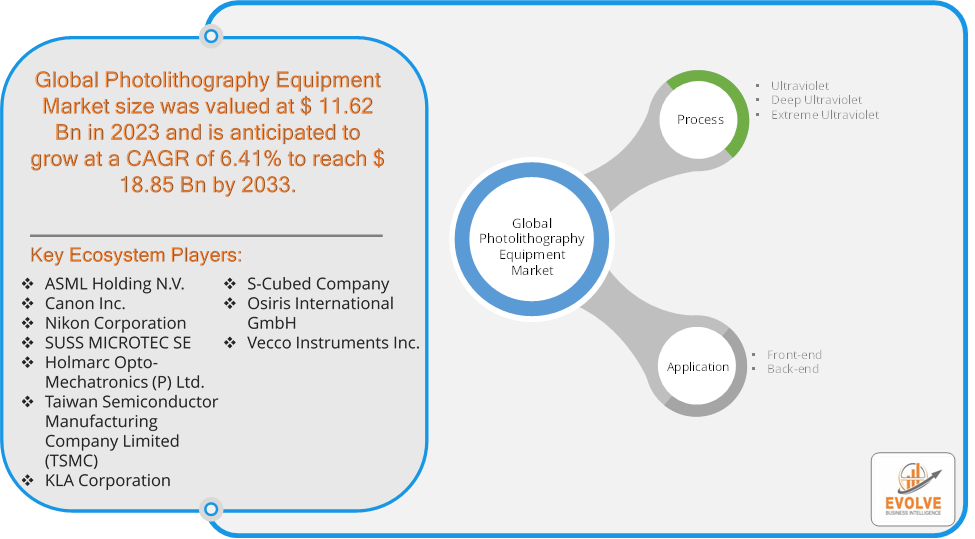
Evolve Business Intelligence has published a research report on the Global Photolithography Equipment Market, 2023–2033. The global Photolithography Equipment Market is projected to exhibit a CAGR of around 6.41% during the forecast period of 2023 to 2033.
Evolve Business Intelligence has recognized the following companies as the key players in the global Photolithography Equipment Market: ASML Holding N.V., Canon Inc., Nikon Corporation, SUSS MICROTEC SE, Holmarc Opto-Mechatronics (P) Ltd., Taiwan Semiconductor Manufacturing Company Limited (TSMC), KLA Corporation, S-Cubed Company, Osiris International GmbH and Vecco Instruments Inc.
 More Information: https://evolvebi.com/report/photolithography-equipment-market-analysis/
Market Highlights
The Global Photolithography Equipment Market is projected to be valued at USD 18.85 Billion by 2033, recording a CAGR of around 6.41% during the forecast period. The Photolithography Equipment Market refers to the global industry centred around the production, distribution, and sale of photolithography equipment used primarily in the semiconductor manufacturing process. Photolithography is a critical step in the production of microchips and other semiconductor devices, involving the transfer of intricate patterns onto a substrate (usually silicon) to create the various layers of a semiconductor wafer.
This market is critical to the semiconductor industry, which in turn is essential for a wide range of modern technologies.
The COVID-19 pandemic had a significant impact on the Photolithography Equipment Market. The pandemic led to temporary shutdowns of manufacturing facilities, particularly in China and other key regions in East Asia, where a significant portion of photolithography equipment components are produced. This caused delays in production schedules and extended lead times for equipment deliveries. Social distancing measures, travel restrictions, and health concerns resulted in reduced workforce availability in manufacturing plants and impacted field services such as installation and maintenance of photolithography equipment. The pandemic accelerated digital transformation across various sectors, driving demand for semiconductors used in consumer electronics, data centers, and telecommunications. This, in turn, boosted demand for advanced photolithography equipment, particularly as manufacturers moved to smaller nodes (e.g., 7nm, 5nm, and below) to meet this demand. As global economies began to recover, the semiconductor industry saw a strong rebound, with surging demand for chips across various sectors. This recovery has led to a corresponding increase in demand for photolithography equipment.
Segmental Analysis
The global Photolithography Equipment Market has been segmented based on Process and Application.
Based on Process, the Photolithography Equipment Market is segmented into Ultraviolet, Deep Ultraviolet and Extreme Ultraviolet. The Ultraviolet segment is anticipated to dominate the market.
Based on Application, the global Photolithography Equipment Market has been divided into Front-end and Back-end. The Back-end segment is anticipated to dominate the market.
More Information: https://evolvebi.com/report/photolithography-equipment-market-analysis/
Regional Analysis
The Photolithography Equipment Market is divided into five regions: North America, Europe, Asia-Pacific, South America, and the Middle East, & Africa. North America, particularly the United States, is a critical region for the development and innovation of photolithography equipment. The U.S. is home to several leading semiconductor companies, including Intel, as well as key equipment manufacturers like Applied Materials and Lam Research. North America’s strong focus on AI, cloud computing, and data centers fuels the need for advanced semiconductor devices, thereby increasing demand for cutting-edge photolithography equipment. Europe is home to ASML, the world’s leading supplier of photolithography equipment, particularly EUV lithography systems. ASML’s dominance in this space makes Europe a critical region for the global photolithography market. The European Union is investing in the semiconductor sector as part of its Digital Compass strategy, aiming to increase Europe’s share of global semiconductor production. This includes funding for new fabs and R&D in photolithography technologies. Asia-Pacific is the largest and most significant market for photolithography equipment, driven by the presence of major semiconductor manufacturing hubs in countries like Taiwan, South Korea, Japan, and China. China is rapidly expanding its semiconductor manufacturing capabilities as part of its “Made in China 2025” initiative, aiming for greater self-sufficiency in semiconductor production. This has led to increased demand for photolithography equipment, including significant government investment in local fabs.


